Sunday, 25 December 2011

Difference between branch and call subroutine instruction


Difference between branch and call subroutine instruction?

              Branch instruction:
  • Every time it is not possible to use line-sequence of instruction, sometime we need breakup in our program according to some condition this is nothing but branching and to perform these branching we require some instruction that is called branch instruction
       Eg:       MOV                    R0,     num1
                   MOV                    R2,     num2
                   CMP           R0,     R1
                   JB .             next
                   Sub            R0,     R1
                   MOV                    R2,     R1
       Next:   Sub            R1,     R0
                   MOV                    R2,     R0
  • Here the task of IB. is it compairs the two Numbers i.e. R0, and R1, if R0, < R1, then it goes to next and execute the instruction otherwise it execute the instructions just next to it.
  • The IB is your branch instruction.
       e.g. : IC, INC, IZ, INZ, IB, INB etc.

       Subroutine instruction:
  • Subrouting instruction is the instruction which is used to call the particular procedure.
  • In your main program we call particular procedure execute that procedure and then again switch to main program.
  • The instruction used for. This called to procedure and getting switch to main program is called subroutine instruction.
Interrupt handling of 68000.

Interrupt handling of 68000.

In 68000 the address of the interrupt handler was placed at 4x interrupt handler number thus if interrupt 3 occurred, you went to address 12 ten, at the address was the address of the handler.
With many different I/O devices that can be interrupt controller. I/O devices are hooked up to the PIC and the PIC is the only device that sends the interrupt.

MOV instruction of 8051

MOV instruction of 8051.

MOV copies the value of operand 2 into operand 1 the value of operand 2 is not affected. Both operand 1 and operand 2 must be in Internal RAM. No flags are affected unless the instruction is moving the value of a bit into the carry bit in which case the carry bit is affected or unless the instruction is moving a value into the PSW register.

Synchronous bus & Asynchronous bus


Synchronous bus:
  • Transmitter and receivers are synchronized of clock.
  • Data bits are transmitted with synchronization of clock.
  • Character is received at constant Rate.
  • Data transfer takes place in block.
  • Start and stop bit are required to establish communication of each character.
  • Used in high – speed transmission.
Asynchronous bus:
  • Transmitters and receivers are not synchronized by clock.
  • Bit’s of data are transmitted at constant rate.
  • Character may arrive at any rate at receiver.
  • Data transfer is character oriented.
  • Start and stop bits are required to establish communication of each character.
  • Used in low – speed transmission.

Volatile memory and NonVolatile memory

Nonvolatile memory: If memory can hold data even if power is turned off, then such type of memory are called nonvolatile memory.

Volatile memory: If memory Remove the data if power is turned OFF, then such type of memory are called volatile memory.

ROM: (Read only memory) and PROM: (Programmable read only memory)


 ROM: (Read only memory)
  • ROM is a read only memory.
  • We can not write anything in it.
  • In this we can use diode, MOS to store the information.
  • Decoder is used to select the address lines
  • OE signal is used to enable the output.
PROM: (Programmable read only memory)
  • PROM is a programmable ROM
  • It is used for permanent storage purpose
  • Once we write something in it then we cannot change it. i.e. it become permanent
  • We can use diode along with fusible link in series with it to store the information
  • We can burns the fuse according to the information stored in it.

Function of signals of 8085.

 Function of signals of 8085.

  (i) HOLD                (ii) HLDA

HOLD and HLDA: HOLD is an active high, input signal used by other controller to request microprocessor about use of address, data and control signals.

The microprocessor in response to HOLD generates a signal to acknowledge the requesting device by HLDA signal. When HLDA is active it indicates that microprocessor has received HOLD request and will relinquish the buses in next clock cycle. The other controller will use buses and upon completion of work will remove HOLD signal, because of this microprocessor will also make HLDA low. The microprocessor takes control of buses half clock cycle after HLDA goes low.

Fetch and execute operation

Fetch and execute operation:
OPCODE fetch cycle: The microprocessor uses this cycle to take the OPCODE of an instruction i.e. fetch OPCODE. In this case, the address of memory location where the OPCODE is stored is given by program counter. This is always the first cycle of any instruction cycle. The OPCODE is taken from memory and transferred to instruction register for decoding and execution.


              The time required to complete this cycle is 4 or 6 T states.

              Operand fetch cycle: In 2 and 3 byte instruction, taking OPCODE, doesn’t complete the instruction fetching; so we require operand fetch cycle. For 2 byte instruction we require two operand fetch cycles. In this cycle the address is given by program counter. But the contents are not transferred to instruction register instead they are stored in temporary registers. The time required to complete the operand fetch cycle is 3 T states.

              Memory read cycle: The microprocessor executes these cycles to read data from memory. The address of memory location is give by instruction. In this case, the program counter is not used, instead, instruction will give address or will specify, where the address is present. IO/M=0.


Memory write cycle: The microprocessor executes these cycles to write data to memory. The address to memory is given by instruction IO/M=0.


I/O read cycle: The microprocessor executes these cycles to read data from I/O device instead of memory. The status of IO/ line is HIGH. The address of port is given by instruction.
I/O write cycle: The microprocessor executes these cycles to write or send data from I/O device. The status of IO/M line is HIGH. The address of port is given by instruction.

Emulator and its uses in the system design.

Emulator is a device computer program, or system that accepts the same inputs and produces the outputs as a given system.
A software application which enables the computer to “emulate’’ a piece of hardware, fooling the computer into thinking that the hardware, such as a CD-ROM, is attached to it. Emulators are often used in situations where there is no CD-ROM present, as in case of some laptops or to test an image of a CD-ROM created by CD burning software such as Nero.

STACK operation in 8085 microprocessor.

STACK operation in 8085 microprocessor.
 
The stack is a reserved area of the memory in RAM where temporary information may be stored. An 8-bit stack pointer is used to hold the address of the most recent stack entry. This location which has the most recent entry is called as the top of the stack.
When the information is written on the stack, the operation is called PUSH. When the information is read from the stack, the operation is called POP. The stack works on the principle of Last in First Out or Fist in Lat Out.

Important features of Motorola 68000 microprocessor.

Important features of Motorola 68000 microprocessor.
Features of Motorola 68000 microprocessors:
The Motorola 68000 is a 32-bit CISC microprocessor.
It includes multiuser microcomputers like the WICAT 150, Tandy TRS – 80 Model 16, and Fortune 32: 16 and single – user workstations.
Multiprocessing control.
Binary coded decimal arithmetic e.g. ABCD and SBCD.
Its software is generally forward with the rest of the line.

Vectored interrupts:

 Vectored interrupts: 
When interrupt request is activated the microprocessor control logic executes ideal machine cycle. During this cycle, it generates starting address of interrupt service routine. These addresses are fixed for different interrupts. This memory address of interrupt service routine is called as vector location and interrupts which use these vector locations are called as vectored interrupts.
                   E.g. TRAP, RST 7.5, RST 6.5, RST 5.5

8085 µP instructions

Function of following 8085 µP instructions with examples (i) SHLD (ii) LDAX
       (i)    SHILD Address:
              Mnemonic : SHLD address
              Algorithm        :         (Address) ← L
                                      (Address + 1) ← H
              Operation       :         (Address) = L
                                      (Address + 1) = H
This instruction copies the contents of registers H and L to the memory location specified in instruction.
The contents of L register are stored at the memory location whose address is specified and the contents of register H to the next memory location.
              No. of bytes    :         3 bytes
              First Byte                 :         Opcode
              Second Byte   :         Low order byte of the address
              Third Byte      : High order byte of the address
              Addressing mode: Direct addressing mode
              Flags               :         No flags are affected.
              Example                   :         SHLD 5648 H.
              (ii)          LDAX Rp:
              Mnemonic                :         LDAX Rp
              Algorithm                 :         A ← (Rp)
              Operation                 :         A + (Rp)
This instruction copies the contents of memory location whose address is pointed by the specified register pair to the accumulator.
              The register Rp can be any valid register pair like BC or DE only.
              The contents of the memory location remain unchanged.
              No. of bytes    :         1 byte
                                                ode of LDAX Rp   
              ddressing mode        :        Register indirect addressing mode
              Flags               :         No flags are affected.

Single chip microcomputer

Single chip microcomputer

It is an abject of the present invention to provide a one chip microcomputer which permit the access time for an external memory to be  equal to that for an internal memory. The one chip microcomputer 10 includes are internal ROM II, control Unit 12, output terminal 13, input terminal 14, control circuit 15.

Role of an emulator in microprocessor:


 Role of an emulator in microprocessor:
  1. It is used to test and debug the hardware and software of an external system, such as the prototype of a microprocessor – based instrument.
  2. Part of the hardware of an emulator is a multiwire cable which connects the host system to the system being developed. A plug at the end of the cable is plugged into the prototype system in place its microprocessor.
  3. Through this connection the software of the emulator allows you to download your object code program into RAM in the system being tested and run it.
  4. Link a debugger, an emulator allows you to load and run programs, examine and change the contents of memory locations, insert breakpoints in the program.

SIM (set interrupt mask)


SIM set interrupt mask is used for interrupts handling in 8085: It implies that the instruction mask the interrupts. However the instruction must be executed in order to use the interrupts.It having the following functions:
  1. To set the RST 7.5, 6.5 and 5.5 interrupts.
  2. To Reset RST 7.5 Flip Flop.
  3. To Implement series I/O transmit D7 bit  to transmit data.

DMA dada transfer:


 DMA dada  transfer:
  1. For some  application, such  as  transferring  dada  bytes to  memory  form  magnetic  or optical  disk, however, the  dada  bytes  are coming  in from  the  disk  faster  then  they  can  be  read in  with  program  instruction. In a case like this we use a dedicated Hardware device called a direct memory access (DMA) controller to manage the data transfer.
  2. The DMA controller temporarily borrows the address bus, data bus, and control bus from the microprocessor and transfer the data by directly from the disk controller to a series of memory location.
  3. A DMA controller can also transfer data from memory to a port.

Instruction queue in 8086 microprocessor.

Function of instruction queue in 8086 microprocessor.
Ans.:      
  The EU is decoding or  executing  an instruction  which does not require  use  of the buses,  the BUI fetches up to six instruction bytes  for  the  following  instructions . the BUI stores  these  prefetched  bytes  in a first –in -irst –out  register  set  called a queue

When  the  EU is ready  for  it’s next  instruction , it  simply  reads  the  instruction   bytes  for  the  instruction  from  the  queue  in the  BUI     

This  is much  faster  than  sending  out  an  address to the system  memory  and  waiting  out  memory  to  send  back  the next  instruction  byte  or  bytes

8251 programmable communication interface chip


Applications of 8251 programmable communication interface chip.
Ans.:
8251 is programmable communication interface. Which is used as Universal Asynchronous Receiver Transmitter. (UART 8251), which is modeled on the peripheral interface device adapter.
     It consists:
  1. a serial transmit block.
  2. a serial receive block.
  3. a CPU interface (I/f) block
  4. 8251 is used as program control device.

Program Counter in 8085 microprocessor

 Requirement of a program counter in 8085 microprocessor.

Program counter hold the address of either the first byte of the next instruction to be fetched for execution or the address of the next by byte of instruction. Which has been completely fetched. In both the cases it gets incremented automatically one by one as the instruction byte get fetched. Also program register keeps the address of next instruction.

Synchronous bus and Asynchronous bus


       Synchronous bus:
  1. In synchronous bus, all devices derive timing information from a common
       clock signal.
  1. Fig. 2 shows the timing diagram for synchronous input transfer.
Fig. 2
  1. At time to, the processor places the device address on the address lines of system but and sets the control lines to perform the input operation, during time t1 – t1, address devices gets the address. At time t1, address devices place its data on the data bus, and at time t2, the processor reads the data lines and loads the data from data bus into its input buffer.
Asynchronous bus:
  1. In this the common clock is eliminated and data transfer on the system bus is achieved by use of a hand shake between the processor and the device being addressed. Here the clock line is replaced by two control signals ready and accept.
  2. Fig. 3 shows timing dig, for asynchronous input transfer.

PSW : PROGRAM STATUS WORD

PSW (program status word) : Program status word refers to the accumulator and flag register, this PSW will store the current data or the content of the accumulator and flag register while execution of program.
              A window editor is a program used for editing the plain text file these type of editor are provided with operating system example of one of window editor is notepad which allow the user to search and replace copy, cut and paste, undo and redo operation and also you will perform importing filtering operation with this notepad text of editor.
              Vi is the full screen editor available with all unix system. Vi is visual editor enable the user to create, edit, and correct source program, Vi makes complete use of the keyboard where pretically every key has function.

Friday, 25 November 2011

DATA STRUCTURES

POINTS TO REMEMBER

1. Data refers to a set of values which may represent some observation from an experiment ,facts,figures gathered systematically for one or more specific purposes.A data is the single unit of values of certain type that have meaning to its user.

2. A file is collection of related records. A record is a collection of related files.A field holds a particular kind of data.

3. Each entity has certain properties also known as its attributes that describes it.Entity set is a collection of entities of same type that share the same properties or attributes.

4. The key which is chosen to uniquely identify a record is called primary key and other key(s) are known as alternate key(s).

5. Information is defined as the processed summarized or organized data which when used by its recipient helps in taking decisions.

6. Data structure is a logical or mathematical model of a particular arrangement or organization of data.An efficient data structure uses minimum memory space and execution time to process the structure as possible.

7. An array is a finite ordered set of homogeneous elements.In computer memory , array elements are stored in contiguous memory locations. Each element of an array has a fixed and unique index .

8. A linked list is a dynamic data structure containing of nodes where each node is composed of data and a pointer to the next node.

9. A stack is a linear data structure in which all insertions and deletions are restricted only at one end called the top of the stack.A stack is often described as LIFO(Last In First Out).For example stack of coins are above the other. The basic operation performed on stack are 'Push' and 'Pop'.

10.Traversing , searching , insertion, deletion , sorting , merging , copying , concatenation are key operations performed on a data structure.

11. (a)An algorithm is a sequence of steps or instructions required to solve a given problem.(b)The analysis of algorithm is based on how much memory an algorithm needs to solve a particular problem is called the space complexity of an algorithm.(c)Measure of time complexity of an algorithm where we disregard certain terms of a function to express the efficiency of algorithm is called asymptotic complexity.

12. A tree is a multilevel data structure that represents a hierarchical relationship between finite set of individual elements called nodes.

13. A graph is a non linear data structure that consists of set of nodes (or vertices ) and set of edges , with each edge going from one node to another .Each edge in the graph depicts a relationship between pair of nodes.

Monday, 7 November 2011

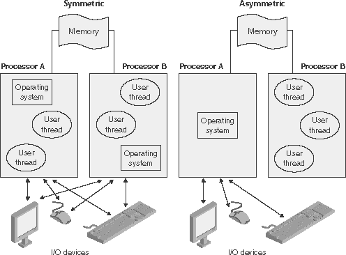
Symmetric vs Asymmetric Multiprocessing


Symmetric vs Asymmetric Multiprocessing

Asymmetric multiprocessing - In asymmetric multiprocessing (ASMP), the operating system typically sets aside one or more processors for its exclusive use. The remainder of the processors run user applications. As a result, the single processor running the operating system can fall behind the processors running user applications. This forces the applications to wait while the operating system catches up, which reduces the overall throughput of the system. In the ASMP model, if the processor that fails is an operating system processor, the whole computer can go down.
Symmetric mMultiprocessing - Symmetric multiprocessing (SMP) technology is used to get higher levels of performance. In symmetric multiprocessing, any processor can run any type of thread. The processors communicate with each other through shared memory.
SMP systems provide better load-balancing and fault tolerance. Because the operating system threads can run on any processor, the chance of hitting a CPU bottleneck is greatly reduced. All processors are allowed to run a mixture of application and operating system code. A processor failure in the SMP model only reduces the computing capacity of the system.

SMP systems are inherently more complex than ASMP systems. A tremendous amount of coordination must take place within the operating system to keep everything synchronized. For this reason, SMP systems are usually designed and written from the ground up.


SIMD(Single-Instruction Stream Multiple-Data Stream)
A graphical representation of a True, Distributed Memory SIMD architecture
                         
 This architecture is essential in the parallel world of computers. Its ability to manipulate large vectors and matrices in minimal time has created a phenomenal demand in such areas as weather data and cancer radiation research.
The architecture consists of a set of identical processing elements (PEs), capable of performing the same operation on different data sets simultaneously. The SIMD allows for a faster and better way to visualize graphics, rendering them almost flawlessly as well as creating them faster.
SIMD architecture is two fold; True SIMD and Pipelined SIMD: 
  • True SIMD
    • Distributed Memory
    • Shared Memory
  • Pipelined SIMD


                                                  MIMD(Multiple Instruction stream, Multiple Data stream)


  •  MIMD has clearly emerges the architecture of choice for general-purpose mutiprocessors.
  •  MIMD machines offer flexibility.
  •  With the correct hardware and software support, MIMDs can function as single user machines focusing on high performance for one application, as multiprogrammed machines running many tasks simultaneously, or as some combination of these functions.
  •  There are two types of MIMD architectures: distributed memory MIMD architecture, and shared memory MIMD architecture.

Short notes on DMA - DIRECT MEMORY ACCESS


CPU BUS SIGNALS FOR DMA TRANSFER


  • The DMA request line is used to request a DMA transfer.
  • The bus request (BR) signal is used by the DMA controller to request the CPU to relinquish control of the buses.
  • The CPU activates the bus grant (BG) output to inform the external DMA that its buses are in a high-impedance state (so that they can be used in the DMA transfer.)
  • The address bus is used to address the DMA controller and memory at given location
  • The Device select (DS) and register select (RS) lines are activated by addressing the DMA controller.
  • The RD and WR lines are used to specify either a read (RD) or write (WR) operation on the given memory location.
  • The DMA acknowledge line is set when the system is ready to initiate data transfer.
  • The data bus is used to transfer data between the I/O device and memory.
  • When the last word of data in the DMA transfer is transferred, the DMA controller informs the termination of the transfer to the CPU by means of the interrupt line.


INTEL 8251A(USART)....(points to remember)


Block diagram of the 8251 USART (Universal Synchronous Asynchronous Receiver Transmitter)


The 8251 is a USART (Universal Synchronous Asynchronous Receiver Transmitter) for serial data communication. As a peripheral device of a microcomputer system, the 8251 receives parallel data from the CPU and transmits serial data after conversion. This device also receives serial data from the outside and transmits parallel data to the CPU after conversion.


                                        operation between a CPU and the device.


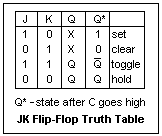
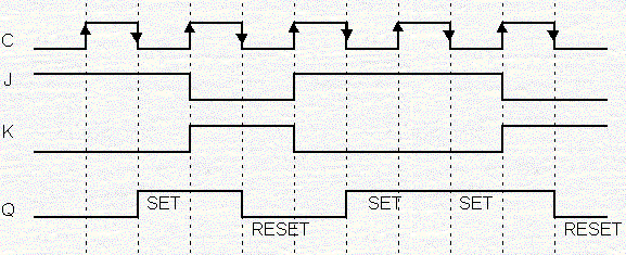
MASTER SLAVE J-K FLIP FLOP(short notes)


CIRCUIT DIAGRAM


Truth Table 


master slave jk flip flop timing diagram


Sunday, 6 November 2011

PARALLEL PROCESSING UNIT

 1. Multiprocessor - is a system having two or more processor and it executes more than one  processes.Main feature of multiprocessor is to share main memory or other resources by all processors.In this one master CPU will control all other processors.The other processor maybe co-processor or input-output processors.

The basic characteristics of multiprocessor system are :
1)This system must have more than one processor.All these processor must have nearly identical processing            
capabilities.

2)All these processor must have common shared memory.

3)Processors share all I/O devices or other resources.

4)The interaction among processor at program level must be defined precisely to have a good and efficient design of hardware for a multiprocessor system.

5)The system configuration can be enhanced at required increments at any point of time.


TYPES OF MULTIPROCESSOR 
(A) Rightly Coupled
(B)Loosely Coupled

Rightly coupled shares common memory and each processor has its own local memory where loosely coupled does not have its own shared memory although each processor will have its own local memory.

The processor used in these types of system are specialized to handle different tasks.This system increases the  overall reliability of system, that means if more than one processor fails, their load is being shared by other processor.

Different schemes used for interconnection of processors and memories are : 

1.) Common Bus : This scheme will provide single bus for interconnection of processors and memory.Its is most effective and simple.
The failure of bus system results in total system failure.The performance of overall system is being limited by data transfer of bus.

2.)Multiple Bus Organisation :This system will provide two or more buses for interconnection of processor and memory.This scheme allows multiple data transfer simultaneously.This will increase reliability without increasing the cost too much.

3.)Crossbar Organisation : This scheme provides interconnection of n processor and n memory modules using switch elements.Switch element is having electronic circuit to provide desired path, it supports priority logic to resolve conflicts.
The hardware implementation is complex as compared to multiple bus organisation.

4.)Multistage Interconnection Network : 

Saturday, 5 November 2011

FILE ORGANIZATION

DIFFERENT FILE ORGANIZATION

File organization basically refers to the logical arrangement of data, which can be organized in a system of records with co-relation between the fields /columns, in a file system.It refers to the way records are physically arranged on a storage device.

TYPES of file organzation:
  1. Heap(unordered) file organization :  the record can be stored where there is storage space available.There  is no fixed order for records.
  2. Sorted file organization: the records are stored in sequential order according to the search key of record. 
    -Sequential(SAM)
    -Line Sequential(LSAM)
    -Indexed Sequential(ISAM)

3. Hashed or Direct : with hashed access or direct a portion of disk space is reserved. Records are placed randomly throughout the file.records are accessed by address that specify their disc location.It has an excellent search retrieval performance, but care must be taken to maintain the indexes.


WHAT IS A FILE ?
A file is a collection of bytes stored in secondary storage device, which is generally a disk of some kind.
The collection of bytes may be interpreted, for example , as characters , words , lines , lines , paragraphs and pages from a textual documents ; fields and records belonging to a data base.
It is simply a machine deciphered storage media, where programs and data are stored for machine storage.


METHODS OF ORGANIZING FILES

1. Sequential Organization : a sequential file contains records organised in the order they were entered.The order of records is fixed.The records are stored and sorted in physical ,contiguous blocks within each block the records are in sequence.
Records in these files can be read or written sequentially.Once stored in the file , the record cant be edited i.e cant be made shorter , longer or deleted. However the record can be updated if the length does not change.
New records will appear at the end of the file.